
Original Link: https://www.anandtech.com/show/1163
Athlon64 Motherboards: First Look at Chaintech, FIC, and MSI
by Wesley Fink on September 23, 2003 1:03 PM EST- Posted in
- Motherboards
At long last, we finally get an opportunity to take a first look at shipping Athlon64 motherboards. The first Athlon64 boards at Anandtech seem almost equally divided between the VIA K8T800 chipset and the single-chip nVidia nForce3 150. Unlike the wide performance differences we see on Athlon between KT600 and the nForce2 Ultra400, performance of VIA and nVidia with Athlon64 is practically a dead heat. Each chipset offers certain unique advantages and weaknesses; but as a buyer, you can evaluate fairly the Athlon64 boards with an eye to features and assume that they will perform similarly – whether they are nForce3 or K8T800. This may change, as we may see one or the other pull ahead over time, but our early testing shows that there is virtually no performance difference between the chipsets.
So where do these new Athlon64 motherboards fit in the new offerings announced today by AMD? The top performer from AMD is called AthlonFX51, and it is more like an Opteron than an Athlon64. This new FX Socket 940 processor, in fact, requires an Opteron motherboard, and at least Registered DDR memory (or Registered ECC) to get it running. The memory you have now is likely unbuffered DDR and it will not work on AthlonFX. FX51 runs Registered or Registered ECC memory in Dual-Channel mode. AMD is projecting small numbers of FX chips and boards going to Computer Enthusiasts until the relaunch of FX early next year in a Socket 939 that can use regular unbuffered memory like you already own.
The new mainstream AMD is Athlon64, a Socket 754 chip that will run your regular unbuffered memory up to DDR400, but in single-channel mode only. The 3 boards for today are all Athlon64 boards tested with AMD’s new Athlon64 3200+. AMD has also announced it will release the Athlon64 in 3400+ speed rating in a few weeks. The upcoming 3400+ runs about the same real speed as the new Athlon64FX51.
The real question is whether Athlon64 can now compete effectively with Intel or outperform the P4 with their mainstream offering. That is a question we hope to answer in these reviews. We also hope to shed some light on whether the Single-Channel Athlon64 is really hampered in competing with the top Pentium 4 chips. The answers may surprise you.
For more in-depth CPU information, please read Anand Shimpi’s Technology Review posted today. He delves deeper into the positioning of the new chips and does in-depth performance comparisons of Athlon64, Athlon64FX, and the Intel P4 chips. If you are confused about the new chips, the speed ratings, or comparative performance, please read Anand’s excellent overview of the new CPU’s. While we will compare performance of the 3 Athlon64 boards with the fastest P4 and Athlon XP offerings in our recent tests, we are comparing performance of 3 motherboards all running an Athlon64 3200+ CPU to the best from our recent Performance tests.
This is the first installment of a larger Athlon64/FX motherboard roundup that will be coming as more boards are delivered to our Lab. With all the significant new hardware and offerings in the market, we will also be updating our benchmark suite to measure and compare better the performance of the newest equipment.
The Chaintech ZNF3-150, FIC K8-800T, and MSI K8T Neo all take different approaches to building a performance motherboard. While the features will be compared, in the end, we are most interested in how the Athlon64 motherboards perform.
nVidia nForce3 Chipset
The Chaintech ZNF3-150 uses the nVidia nForce3 chipset. We covered basic features of the nForce3 in our Athlon64 Preview. Since this will be your first look at nForce3 compared to other solutions, we will talk about basic features of the nForce3.One of the most exciting, and also controversial, features of the Opteron/Athlon64 is AMD’s decision to include the memory controller on the CPU. There are tremendous potential speed advantages to this solution, but the complexity of manufacturing also increases significantly. This can dramatically lower yields, which are becoming increasingly important in a competitive CPU environment. For a chipset maker, the move of the memory controller to the CPU itself means the chipset design is much simplified. In fact, about half of the requirements of the supporting chipset are eliminated, which allows a much simpler design — even the possibility of a single chip solution instead of the customary North and South bridges.
nVidia’s nForce3 PRO is the only one of the Opteron/nForce3 chipsets in a single-chip package. Both VIA K8T800 and SiS755, use the more familiar Northbridge/Southbridge arrangement. Key Features for nForce3 PRO are:
The Athlon64 and Athlon64FX CPU use Hypertransport as their method for internal communications. While these and the Opteron are the first AMD processors to use Hypertransport, this architecture is something nVidia has used in their nForce series since their original nForce chipset.
- Single-Chip Solution — Revolutionary single-chip solution designed for the AMD Opteron CPU enables higher-quality, full-featured motherboards and delivers maximum performance with the lowest latency. The single-chip design also means less power consumption and less heat dissipation.
- Dual-Channel DDR400 Memory — Our reference board includes full support for Dual-Channel DDR ECC memory, and the Athlon64 version will also support non-ECC memory.
- Integrated SATA/IDE Raid — Provides support for RAID 0, RAID 1, and RAID 0+1, enabling the highest disk data transfer rates for highest system and application performance, and the highest performance fault tolerant solution for maximum data integrity. NVIDIA RAID supports both SATA and ATA-133 disk controller standards.
- Enterprise-Class Networking — Delivers the essential manageability features required by IT professions while maintaining the highest level of reliability, quality, and performance. Also delivers the highest throughput for network transfers and lower CPU utilization, resulting in lower total cost of ownership.
- 64-Bit Architecture — NVIDIA nForce3 Pro provides advanced processing capabilities and system innovations for the new 64-bit AMD processor architecture.
More information on nForce3 PRO is available at http://www.nvidia.com/page/nforce3.html.
If you are interested in learning more about the features and architecture of Opteron and Athlon 64, you can access Anand’s excellent 3-part article.
VIA K8T800 Chipset
The FIC K8-800T and MSI K8T Neo are built with the VIA K8T800 chipset. Since this is our first look at a board built on the K8T800 chipset, it is important to have a basic understanding of the features of the chipset compared to others for the Athlon64 processor.One of the most exciting, and also controversial, features of the Opteron/Athlon64 is AMD’s decision to include the memory controller on the CPU. There are tremendous potential speed advantages to this solution. For a chipset maker, the move of the memory controller to the CPU itself means the chipset design is much simplified. In fact, about half of the requirements of the supporting chipset are eliminated, which allows a much simpler design — even the possibility of a single chip solution instead of the customary North and South bridges.
VIA chose to use a traditional North Bridge/South Bridge design instead of a single chip solution. The following Features and Benefits of the K8T800 come directly form VIA literature.
Key Features of VIA K8T800
- Supports full range of AMD Opteron/Athlon64 processors
- Hyper8 Technology enables 16-bit/1.6GHz HyperTransport processor-to-chipset link
- Support for AGP 8X/4X
- V-Link 533 MB/sec high bandwidth North/South Bridge interconnect
- Support for VIA Vinyl 5.1 & Vinyl Gold 7.1 Multichannel Audio Suite
- Serial ATA support for up to 4 devices
- Integrated V-RAID with RAID 0, RAID 1
- Parallel ATA133/100/66 support for up to 4 devices
- Support for up to 8 USB 2.0/USB 1.1 ports, UHCI compliant
- Support for VIA Gigabit Ethernet controller & Integrated 10/100 Fast Ethernet
- Integrated MC'97 Modem
- Advanced power management capabilities including ACPI/OnNow
- 578-pin BGA North Bridge
- 539-pin BGA VT8237 South Bridge
Benefits of VIA K8T800
VIA Hyper8™ Technology
VIA's unique Hyper8 technology eliminates noise on the HyperTransport link between the processor and chipset, enabling the industry's only full-speed, full-spec 16-bit/1.6GHz implementation of the processor-to-chipset HyperTransport link.
VIA Modular Architecture Platform
To best exploit the rapid pace of innovation in the PC industry, particularly with reference to I/O technology, VIA have opted for a classic North/South Bridge configuration allowing for the most scalable mainboard design, enabling new functionality to be integrated in an expedient and practical manner, thus providing the fastest time to market with new features and system performance enhancements.
Native Serial ATA/RAID Support
The VIA DriveStation™ Controller Suite with native dual channel Serial ATA/RAID controller, provides direct support for two 150MB/s Serial ATA devices and its unique SATAlite™ interface expands support for two additional SATA devices. The V-RAID controller features native RAID 0 & RAID 1. The user friendly V-RAID software interface enables easy disk array configuration and management.
VIA Vinyl Multichannel Audio Suite
Delivering rich, warm surround sound at resolutions as high as 24/96 through up to six- or eight-channel outputs, the VIA Vinyl Audio 5.1 surround sound and VIA Vinyl Gold Audio 7.1 surround sound enables crisp, clear performance, representing the highest levels of audio quality in a mainstream integrated or onboard solution.
Unified VIA Hyperion 4in1 Drivers
VIA's unified approach to drivers has been established for eight generations of chipsets, allowing end users to benefit from seamless hardware and software compatibility.
VIA has made quite a point lately in literature and press releases of the fact that they are the only chipset to support fully the full-speed 800Mhz (1.6GHz) Hypertransport bus. This is certainly true. A full 800MHz HT bus requires very low noise circuits, and VIA claims that others cannot yet implement 800 Hypertransport because of excessive circuit noise.
nVidia has a very different explanation, and they believe their single-chip solution is superior because it eliminates the 533 Mb/sec "bottleneck" that exists between VIA's 2-chip Northbridge and Southbridge solution. It is true that VIA runs a 3.2GHz uplink/downlink, while the nVidia nForce3-150 runs a 2.4GHz downlink and 1.2GHz uplink. However, nVidia says VIA's 3.2GHz must then be crammed into the 533mb/sec link between the north and south bridges which negates any advantage a 3.2GHz design might have. The nVidia nForce3-150 was designed with a 16-bit downlink/8-bit uplink running at 600MHz DDR (1.2GHz effectively) in a SINGLE chip that is connected to the CPU with a 3.6GHz connection. NVIDIA claims this is a much more efficient and faster solution, and they are confident that current nForce3-150 chipsets will not be penalized in performance as a result of the 600MHz HT speed.
nVidia has also announced that their upcoming nForce3-250 chipset, which we understand will likely be introduced with Socket 939 solutions, will run at the full 800MHz Hypertransport speed.
As we will see in benchmarks, the practical effect of 600MHz vs. 800MHz Hypertransport on performance of desktop Athlon64 machines is nil at present. However, as we see Athlon64/Opteron chipsets mature, we may see that this has a greater impact on future performance. More information on VIA K8T800 is available at http://www.viatech.com/en/k8-series/k8t800.jsp.
If you are interested in learning more about the features and architecture of Opteron and Athlon 64, you can access Anand’s excellent 3-part article.
Chaintech ZNF3-150: Athlon64 with Every Option
The Chaintech ZNF3-150 is one of the more interesting packages that we have seen in quite a while, since it creates a new definition for high-end motherboards. We have seen this from Chaintech before, with the remarkably complete 7NJS-ZENITH and 7NJS-ZENITH Ultra. The ZNF3-150 certainly continues that tradition of providing every option that the enthusiast could want and then some. DFI and Soyo have produced similar packages with their LANParty and Platinum series boards, but Chaintech has a slightly different slant. It is clear that their aim with this Athlon64 board is the Performance enthusiast.This time around, Chaintech has concentrated on board options that can affect performance, which include using 4-phase power instead of the 2- and 3-phase designs that we see on other Athlon64 boards. They have also added a copper heat-pipe cooling solution to the power transistors, which they call Radex. The performance options are new, but the rest of the package mirrors the more recent Chaintech packages and includes round cables, audio riser card, a front bay with ports and flash-card reader, and every option that you can think of including a Chaintech screwdriver.
While we have to give Chaintech the award for the most intriguing motherboard package that we have seen in quite a while, our main interest is whether all this attention to performance enhancement will really make a difference. This is, after all, the Athlon64 single-channel version of the new processor, and AMD is also introducing the “Enthusiast” version of this CPU, called Athlon64FX, that will run at a little faster clock speed and support dual-channel memory. Why, then, have an enthusiast Athlon64 board?
The answer is really very simple, and we think Chaintech is right on track with this solution. Athlon64FX is very expensive as it is launched, and the costs are not just the higher priced CPU. FX is basically an Opteron in a different costume, and as a result, it requires the use of at least Registered DDR memory or Registered ECC DDR memory. You cannot use your common unbuffered DDR400 or DDR500 with an Athlon64FX. New Registered Dual-Channel DDR400 memory is very hard to find at present. You also will have, initially at least, a much smaller selection of motherboards from which to choose. We currently have an Asus SK8N that we will be benchmarking with an Athlon64FX, but there are very few FX boards available.
This will all change early next year, when Socket 939 will be introduced. This will be Athlon64FX designed for regular unbuffered Dual-Channel memory. However, until that happens, the decision to go for Athlon64FX will be a very expensive one, also tempered by the limited availability of Athlon64FX chips for the next few months. For those reasons, Chaintech made a very wise decision in producing the ZNF3-150. Performance truly comparable to 3.2GHz processors and the promise of even faster Athlon64 CPUs will be a breath of fresh air for most, and many will be looking for a full-featured top-performing motherboard to go with their new Athlon64.
Chaintech ZNF3-150: Packaging & Board Layout
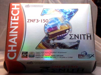
The foil-faced box is about twice as thick as a regular motherboard box to contain all the extras with the ZNF3-150. The manual and quick setup reference sheet are both very complete and well done.
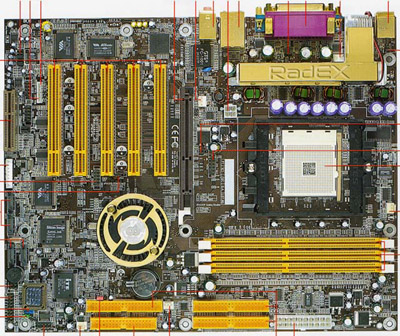
Layout of the Chaintech is very close to ideal. Placement of IDE/Floppy ports is in the preferred upper right position behind the DIMM slots. The 5 PCI slots are located in the 1 through 5 positions, and yet clearance was considered. The AGP and DIMM slots do not interfere with each other, so upgrading or adding memory is very easy. There are 2 areas, however, that could be improved. First, the location of the 12V 4-pin power cable to the left of the CPU and about midline of the board requires careful routing of the cable to not disturb the CPU. It would be better if it were higher on the board, near the top edge. Also, the dedicated multimedia card draws mixed reviews. The concept is great, but the location at the very bottom left of the motherboard makes feeding any connectors from optical drives difficult at best. You will likely need an extension if you want to connect the output from your optical directly to the Multimedia card. Other than those 2 areas, the board is well laid-out and shows careful attention to detail.
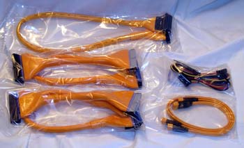
A full selection of round IDE cables, floppy cables and matching SATA cables are provided.
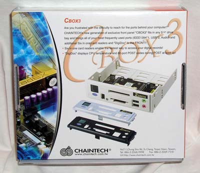
The included Cbox3 fits in a 5-1/4” front bay and provides USB, firewire, SmartDoc system temperature readouts, front audio connectors, and slots for reading a variety of flash cards from your digital equipment.
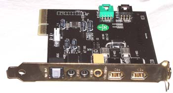
The multimedia riser card includes a full variety of input/output ports and speaker connections for the on-board 24-bit Envy audio.
Chaintech ZNF3-150: Basic Features
| Motherboard Specifications | |
| CPU Interface | Socket-754 |
| Chipset | nVidia nForce3-150 Single Chip |
| Bus Speeds | 200 MHz to 400 MHz (in 1 MHz increments) |
| Core Voltages Supported | Default, 1.45V to 1.70V (in 0.025V increments) |
| AGP Voltages Supported | Default, 1.6V to 2.2V (0.1V increments) |
| DRAM Voltages Supported | Default, 2.7V to 2.9V (in 0.1V increments) |
| Chipset Voltage | Default, 1.7V to 1.9V (in 0.1V increments) |
| Memory Slots | 3 x 184-pin DDR DIMM Slots Support to 2Gb DDR400/333/266/200 |
| Expansion Slots | 1 AGP 8X Slot 5 PCI Slots 1 Chaintech MultiMedia |
| Onboard RAID | Silicon Image Sil3224 supports up to 4 SATA drives in Raid 0/1/5/10 configurations |
| Onboard USB 2.0/IEEE-1394 | Six USB 2.0 supported through nForce3 VIA VT6306 IEEE-1394 Controller for 3 ports |
| Onboard LAN | Broadcom GigaLAN |
| Onboard Audio | VIA Envy 24PT 1.1 channel 24-bit |
| Onboard Serial ATA | Six IDE drives provided by 3 IDE connectors via nForce3-150 Four SATA connectors via Sil3224 Controller |
| BIOS Revision | 9/18/2003 |
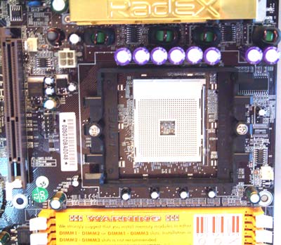
The “cage” for attaching the Heatsink/Fan for the Athlon64 is much more robust than the small, easily-broken lugs for Socket A Athlon. The holder is attached with 2 screws to a back plate, which reinforces the whole socket area. The HSF that we have seen have large clips which are connected, and then an arm for final tightening that is pushed down and locks to the holder. In actual use, the new HSF assembly is much better than what we thought it would be. It is a decent solution that should allow very effective cooling solutions to be attached to Athlon64 processors.
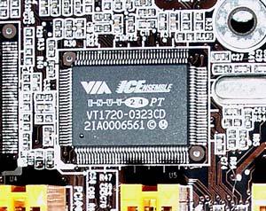
Chaintech uses the VIA Envy24PT, a 7.1 multi-channel format integrated audio controller. 24-bit audio resolution is supported as well as 96KHz sampling rates for digital connections. The VIA Envy24PT also supports up to 8-channel outputs enabling support for Dolby Digital EX and DTS ES DVD-Video soundtracks. It is clear from the high-end specs of Envy24 and the MultiMedia riser that Chaintech intends the ZNF3-150 on-board audio to make no apologies to any one.
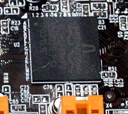
Gigabit LAN is provided by the Broadcom 10/100/1000 chip.
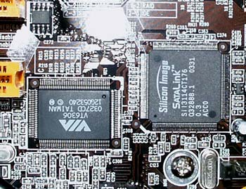
3 firewire ports are provided by the VIA VT6306 chip. Silicon Image Sil3114 supports up to 4 Serial ATA connections with RAID 0/1/0+1. Chaintech claims Raid 0/1/5/10 compatibility in their specifications.
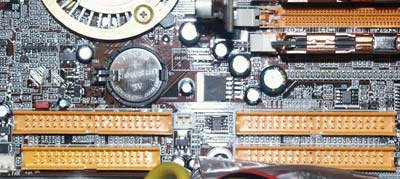
The Single-Channel nForce3-150 adds control for up to six IDE devices, up to ATA133, connected to the 3 IDE sockets.
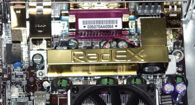
The ZNF3-150 uses a very robust 4-phase power instead of the more typical 2- and 3-phase seen on other Athlon64 boards. The Radex copper heat-pipe/active fan system cools the power transistors used in the 4-phase power system.

The color coding that is used throughout the ZNF3-150 is continued onto the IO deck on the rear. The slots you see are the output from the Radex heatpipe and fan system that cools the power transistors.
Chaintech ZNF3-150: BIOS and Overclocking
Chaintech uses the familiar Phoenix-Award BIOS. As detailed in Basic Features, a full range of overclocking options are available including adjustable CPU voltage, memory voltage, AGP voltage , and Chipset voltage. As we have seen on all nVidia chipsets, AGP/PCI clock can be fixed for maximum overclocking. The latest 9/19/03 BIOS adds a full range of manual memory timing selections to the Advanced chipset section.The Athlon64 has a full heatspreader like Pentium4, so it would appear that any multiplier adjustments would have to be available on the board or in the BIOS. There are no selections for multiplier adjustments in the BIOS. We also did not find Multiplier Adjustments on any of the other Athlon64 boards that we examined.
FSB Overclocking Results
One of the questions about Athlon64 that everyone has asked is whether it will support overclocking that will be competitive to the ranges offered by Intel 800FSB processors. Our 3200+ chip, with a default FSB setting of 200, was able to boot into Windows as high as 236FSB. We found that we could achieve stable operation at 230FSB by lowering the memory setting to 333, so we were running near DDR400 at a 230 setting. The highest stable 1:1 overclock (DDR400 memory setting) that we could achieve was at 222FSB.| Front Side Bus Overclocking Testbed | |
| Processor: | AMD Athlon64 3200+ (2.0GHz) |
| CPU Voltage: | 1.525V (default) |
| Cooling: | Cooler Master Athlon64 HSF |
| Memory: | 2 x 512MB Mushkin PC3200L2 at 2-2-2-6 timings |
| Power Supply: | Powmax 350W |
We are looking at our first samples of Athlon64 boards, but for those who wish to overclock their systems, you will be pleased to find that there is some decent headroom for overclocking. However, without multiplier adjustments in BIOS or any visible means to change multipliers on the heatshield covered chip, it is critical that the BIOS offer fixed ratios for AGP/PCI for best overclocking results. The Chaintech ZNF3-150 has the ability to fix the AGP/PCI frequency.
Chaintech ZNF3-150: Memory Testing
The ZNF3-150 has 3 memory slots, but they are a bit unique. Slot one can handle up to 1GB of memory, and slots 2 and 3 together can handle an additional 1 GB. Chaintech recommends that memory be placed in slots 1 and 2 or 1 and 3, but not in 2 and 3. We did all testing with 2 sticks of Mushkin 512Mb PC3500 L2 memory in slots 1 and 3 and made no attempt to fill all 3 slots.Front Side Bus Stress Test Results:
We performed stress tests on the ZNF3-150 in these configurations:1. Chipset and motherboard stress testing, conducted by running the FSB at 230 MHz with Mushkin PC3500 L2 at 5:4 memory ratio (DDR368) with 2 x 512MB double-bank DIMMs at 2-2-2-6 timings.
2. Memory stress testing, conducted by running Mushkin PC3500 L2 RAM at 400MHz with all DIMM 1 and 3 filled.
We ran a full range of stress tests and benchmarks to ensure that the Chaintech ZNF3-150 was absolutely stable at standard DDR400 speed and at overclocked FSB speed. We ran several tasks — data compression, various DX8 and DX9 games, and apps like Word and Excel — while Prime95 was running in the background. Finally, we ran our complete benchmark suite, which includes ZD Winstone suite, Unreal Tournament 2003, SPECviewperf 7.0, and Gun Metal Benchmark 2.
Memory Stress Test Results:
The memory stress test is very simple, as it tests the ability of the Chaintech ZNF3-150 to operate at its officially supported memory frequency (400MHz DDR) at the lowest supported memory timings that our Mushkin PC3500 Level II can achieve:| Stable DDR400 Timings (2/3 banks single-channel populated) |
|
| Clock Speed: | 200MHz |
| Timing Mode: | Manual |
| CAS Latency: | 2.0 |
| Bank Interleave: | Auto |
| RAS to CAS Delay: | 2T |
| RAS Precharge: | 6T |
| Precharge Delay: | 2T |
| Command Rate: | 1T |
The ZNF3-150 had no problem handling any of the benchmarks or stress tests at 2-2-2-6 memory timings. It is worth mentioning that the “Auto” setting in BIOS set memory timings of 2-3-3-6 with our Mushkin memory. While 2-2-2-6 timings, set manually, did provide slightly better performance, the real difference between Auto 2-3-3-6 and manual 2-2-2-6 timings was extremely small. For most situations, Auto timings will provide excellent stability and speed.
FIC K8-800T: Great Athlon64 Features in a Basic Board
FIC is a very large supplier of OEM motherboards, which means they manufacture many boards that you will see in the market under other brand names. Their own Athlon64 offering, the K8-800T is a pleasant, excellent-performing board based on the VIA chipset. In most comparisons, it would be considered loaded with features, since it includes 8 USB 2.0 ports, on-board LAN, 6-channel audio, a Digital I/O bracket, and 2 firewire ports. It is only in comparison to the Chaintech ZNF3-150 and MSI K8T Neo that we would consider the feature set more basic. The FIC will more likely sell at the mid to low-mid range of Athlon64 motherboards, and it certainly will offer a lot of value at that price. It would be an excellent choice for building a top-performing Athlon64 system, especially if you have a budget and money is an object.The design of the FIC K8-800T is extremely flexible. FIC can add options for a full-featured board, or manufacture without certain features for a price point. Even the on-board LAN is designed so that either a 10/100 or GigaLAN can be dropped in. The advantage of FIC’s approach is that the board is adaptable to whatever direction might develop in the Athlon64 market. However, this means that the buyer needs to check on-board features carefully, since they will likely see several versions of the FIC available from different sources. Just make sure to check the features list of the K8-800T before you buy and then you will not be disappointed in the motherboard.
FIC K8-800T: Packaging & Board Layout
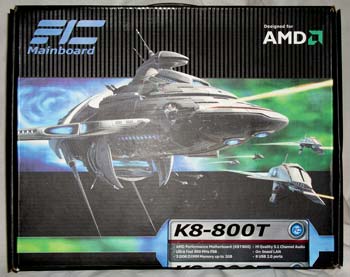
FIC packages the K8-800T in their new black AMD box.
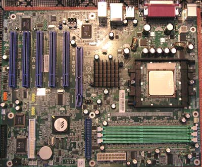
Basic layout of the board is good, with plenty of room around the CPU socket and a large passive heatsink on the VIA K8T800 Northbridge. The DIMM slots clear the AGP slot so memory changes and upgrades are painless. Our only complaint is the floppy connector at the lower bottom of the board, which is a difficult location in some cases. We also prefer the IDE connectors on the right edge of the board above midline (right of the DIMM slots) in most board designs. There must be a reason for the IDE slots to be scattered across the lower right behind the IDE/AGP slots, but it certainly is not for the convenience of the end-user.
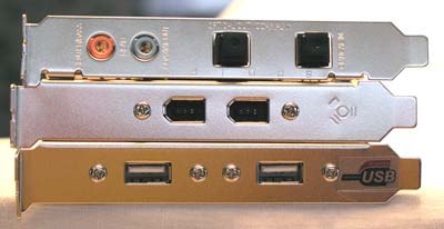
FIC included brackets for Digital I/O with both Optical in and out connectors. Also included were brackets for 2 Firewire ports and 2 additional USB 2.0 ports. 4 USB ports are already included on the rear IO connections.

Rear IO provides 2 PS2 ports, 2 serial ports, 4 USB 2.0, onboard LAN, and audio outputs for the onboard Realtek ALC655 audio.
FIC K8-800T: Basic Features
| Motherboard Specifications | |
| CPU Interface | Socket-754 |
| Chipset | VIA K8T800 Northbridge VIA 8237 Southbridge |
| Bus Speeds | 200 MHz to 232 MHz (in 1MHz increments) |
| AGP/PCI Speeds | Disabled, 66.0, 75.4** |
| Core Voltages Supported | ** |
| AGP Voltages Supported | Default, 1.5V to 1.8V (0.1V increments) |
| DRAM Voltages Supported | Default, 2.5V to 2.8V (in 0.1V increments) |
| Chipset Voltage | None |
| Memory Slots | 3 x 184-pin DDR DIMM Slots Support to 2GB DDR 400/333/266 |
| Expansion Slots | 1 AGP 8X Slot 5 PCI Slots |
| Onboard RAID | VIA 8237 supports 2 SATA drives in Raid 0/1 configurations |
| Onboard USB 2.0/IEEE-1394 | 8 USB 2.0 supported through VIA8237 VIA VT6307L Firewire for 2 ports |
| Onboard LAN | Realtek 8100C 10/100 |
| Onboard Audio | Realtek ALC655 AC’97 6-Channel |
| Onboard Serial ATA | Four IDE drives provided by 2 IDE connectors by VIA 8237 Two SATA connectors by VIA 8237 |
| BIOS Revision | Pre-Release |
| ** The tested board had no provisions for Fixed or Locked AGP/PCI or Core Voltage. However, FIC indicates shipping BIOS will supply both. Values for “Async AGP Clock Control” are from K8-800T Manual. | |
There is plenty of room around the Socket 754 “cage” for attaching the Heatsink/Fan. The capacitors to the rear of the socket are tall, and could possibly interfere with mounting massive heatsink/fans on the K8-800T.
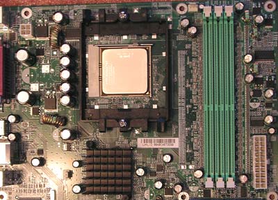
FIC has located the 24-pin ATX and 4-pin 12V connectors in almost ideal locations. The ATX is preferred right above midline location, which makes routing the bulky 24-pin cable much easier in most cases. The 12V connector is preferred to the right of the CPU, but FIC chose the left of CPU location. This location still works fine if, as FIC did with the K8-800T, the location is high on the board. The top left position used by FIC worked well.
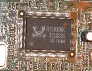
10/100 LAN is provided by the Realtek 10/100 chip. As stated in the manual, FIC can easily provide Gigabit LAN on future boards.
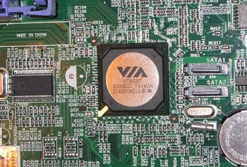
The VIA 8237 Southbridge provides support for 8 USB and 2 SATA ports in addition to standard I/O offerings.
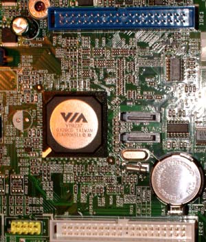
The two SATA connectors are driven by the VIA 8237 and offer standard SATA operation as well as RAID 0/1.
FIC K8-800T: BIOS and Overclocking
FIC uses the familiar Phoenix-Award BIOS. A full range of overclocking options are available including adjustable CPU voltage, memory voltage, and AGP voltage. We were more than a bit concerned that there were no options in the pre-release BIOS for vCore, Memory Timings, or the very important AGP/PCI lock, even though these features are described in the manual. FIC assures us that these features will be available in the shipping version of the BIOS.As with other tested Athlon64 boards, we did not find a provision for multiplier adjustments in the BIOS. This makes the AGP/PCI lock particularly important, since high settings of the FSB will be the only available means of overclocking — the same as what we currently see on the Pentium 4 chips.
FSB Overclocking Results
Without a PCI/AGP lock in the pre-release BIOS, we made no serious attempt to overclock the K8-800T. We will explore this important subject with a shipping FIC BIOS in our upcoming Athlon64 motherboard roundup.FIC K8-800T: Memory Testing
The K8-800T has 3 memory slots, but they are a little unusual, like those found on the Chaintech ZNF3-150. According to a note in the FIC manual:If you use double-sided PC3200 DDR DIMM, only DIMM1 socket is allowed. IF single-sided PC3200 DIMM is used, either DIMM2 or DIMM3 is allowed, but not both at the same time.
These interesting memory requirements will be explored further in future Athlon64 reviews and the Athlon64 motherboard roundup. It looks as if the DIMM slot precautions on the VIA K8T800 based FIC are similar to those on the Chaintech nForce3 board. We can only say that we had run all memory tests and benchmarks with 2 DS PC3500 DIMMs in slots 1 and 3, and we had no trouble at all with board stability. We made no attempt to check 3 filled slots in our memory stress tests, as we really didn’t want to push it with a pre-release BIOS, which are often more fragile than production BIOS.
Front Side Bus Stress Test Results:
We performed stress tests on the FIC K8-800T by running Mushkin PC3500 L2 DS DDR at 400MHz with DIMMs 1 and 3 filled.We ran a full range of stress tests and benchmarks to ensure that the FIC K8-800T was absolutely stable at standard DDR400 speed. We ran several tasks — data compression, various DX8 and DX9 games, and apps like Word and Excel — while Prime95 was running in the background. Finally, we ran our complete benchmark suite, which includes ZD Winstone suite, Unreal Tournament 2003, SPECviewperf 7.0, and Gun Metal Benchmark 2.
The FIC showed no stability problems in our stress tests with both banks filled with double-bank DIMMs at stock 400 speed.
Memory Stress Test Results:
The memory stress test is very simple, as it tests the ability of the FIC K8-800T to operate at its officially supported memory frequency (400MHz DDR) at the lowest supported memory timings that our Mushkin PC3500 Level II can achieve. Despite dire warnings in the FIC manual, we ran 2 DS DIMMs at DDR400 as follows:| Stable DDR400 Timings (2/3 banks single-channel populated) |
|
| Clock Speed: | 200MHz |
| Timing Mode: | Auto |
| CAS Latency: | 2.0 |
| Bank Interleave: | Auto |
| RAS to CAS Delay: | 3T |
| RAS Precharge: | 6T |
| Precharge Delay: | 3T |
| Command Rate: | N/A |
Since there were no memory timings available in our pre-release BIOS, we were forced to run Memory Timings at “Auto” settings. CPU-Z reported “Auto” was setting memory timings at 2-3-3-6. Please keep in mind that when comparing benchmarks, the FIC tests were run at slower memory timings than Chaintech or MSI. While 2-2-2-6 timings, set manually, did provide slightly better performance, the real difference between Auto 2-3-3-6 and manual 2-2-2-6 timings was small. For most situations, Auto timings will provide excellent stability and speed.
MSI K8T Neo: Athlon64 with Dynamic Overclocking
MSI takes the approach of “everything you could ever want” in their top-line K8T Neo motherboard. As MSI has done in the past, they will likely market a top full-featured K8T Neo series board, and then market one or two scaled down versions of the same board with fewer features and at lower cost. MSI is also using the VIA K8T800 chipset to power its top Athlon64 board.If we were looking at the MSI board in isolation, we could not help but be impressed with the array of options and features that MSI lavishes on this board. In addition to standard fare with the VIA 8237 Southbridge (2 SATA Raid, 8 USB 2.0, and ATA133 IDE), MSI has added Gigabit LAN, Promise 20378 controller (2 SATA plus 1 ATA133), firewire ports, D-Bracket diagnostics, 5.1 audio with rear deck connection for all speakers plus Coax/Optical SPDIF, and round red cables to match the red motherboard. The package is impressive, and it is only when it is compared to a package like the Chaintech ZNF3-150 that it looks a little less than spectacular.
MSI is one of the largest motherboard manufacturers in the world, and recently they have been using a new technology called Dynamic Overclocking with their top-end boards. The K8T does have Dynamic Overclocking, with selectable values to 10% overclock, and the important ability to defeat the D.O.T. and set values yourself if you prefer your own overclocking recipes. All-in-all, the MSI K8T Neo has an impressive array of features, ports and options.
MSI K8T Neo: Packaging & Board Layout
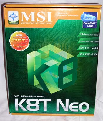
MSI packages the K8T Neo in a foil box for the K8T Neo series, much like others we have recently seen from MSI. You’ll have no trouble finding it in person with the bight green color announcing that this is a board for AMD.
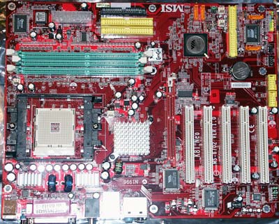
Basic layout of the board is good, with low profile DIMMs used near the Athlon64 “cage” to provide clearance for even massive heatsink/fans. There is a large passive heatsink on the VIA K8T800 Northbridge. The DIMM slots clear the AGP slot, so memory changes and upgrades are painless. The IDE and floppy slots are in our preferred location, right of the DIMM slots and above the midline of the board. So, there should be no problem with snaking cables in most case designs. As we often see with 3rd IDE connectors, it is located near the bottom right of the board. Since this IDE connector will only be handling hard drive connections, this location is usually fine for HD only ports. The 4 SATA connectors are also at the lower right of the board. Our only complaint is the 4-pin 12V connector, which is located to the left of the CPU near middling. This means that you will need to route your 12V power connection around your CPU and down the board, while trying not to interfere with the CPU and HSF.
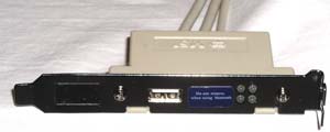
MSI includes their standard D bracket with extra USB ports and the 4 diagnostic LEDs.

The rear panel of the K8T Neo contains an amazing number of ports. Standard ports include the standard PS2 ports, parallel, and just 1 serial port. To this MSI adds 4 USB 2.0, Gigalan, both standard and mini Firewire, Coax SPDIF, Optical SPDIF, and 5 mini-plugs for connecting speakers, mic, and line.
MSI K8T Neo: Basic Features
| Motherboard Specifications | |
| CPU Interface | Socket-754 |
| Chipset | VIA K8T800 Northbridge VIA 8237 Southbridge |
| Bus Speeds | 190 MHz to 280 MHz (in 1 MHz increments) |
| AGP/PCI Speeds | None** |
| Core Voltages Supported | +3.3%, +5%, +6.6%, +8.0%. +10%, +11%, +15% |
| AGP Voltages Supported | Auto, 1.55V to 1.85V (0.05V increments) |
| DRAM Voltages Supported | Auto, 2.55V to 2.85V (in 0.5V increments) |
| Chipset Voltage | None |
| Memory Slots | 3 x 184-pin DDR DIMM Slots Support to 2GB DDR 400/333/266 |
| Expansion Slots | 1 AGP 8X Slot 5 PCI Slots |
| Onboard RAID | VIA 8237 supports 2 SATA drives in Raid 0/1 configurations Promise 20378 supports 2 SATA + 2 IDE device in RAID 0/1/0+1 |
| Onboard USB 2.0/IEEE-1394 | 8 USB 2.0 supported through VIA8237 VIA VT6307L Firewire for 2 ports |
| Onboard LAN | Realtek 8100C 10/100 |
| Onboard Audio | Realtek ALC655 AC’97 6-Channel |
| Onboard Serial ATA | Four IDE drives provided by 2 IDE connectors by VIA 8237 Two SATA connectors by VIA 8237 2 SATA+ 2 IDE by Promise 20378 |
| BIOS Revision | 1.0 |
| ** The tested board had no provisions for fixed AGP/PCI. However, shipping BIOS may or may not supply this option. MSI states that they hope to provide AGP/PCI fix option in the next 2 to 3 weeks. | |
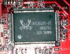
Gigabit LAN is provided by the Realtek 8110S 10/100/1000 chip.
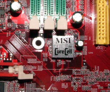
MSI’s proprietary CoreCell provides “Dynamic Overclocking”.
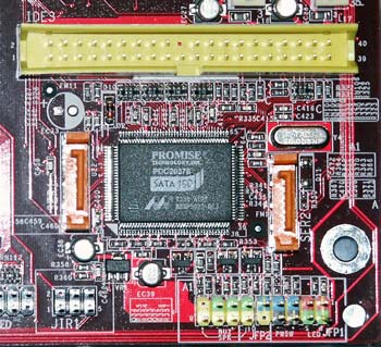
In addition to the two SATA connectors driven by the VIA 8237 Southbridge, MSI adds the Promise 20378 controller for 2 additional SATA ports and a 3rd IDE connecor supporting RAID 0/1/0+1.
MSI K8T Neo: BIOS and Overclocking
MSI uses AMI BIOS on the K8T Neo, but the look and feel of the BIOS options in this AMI BIOS are almost exactly like a Phoenix-Award BIOS. A full range of overclocking options are available, including adjustable CPU voltage, memory voltage, and AGP voltage. A full range of memory timings are available, including the ability to set CAS 2, 2.5, or 3.0 timings. Memory Timings worked well. We could find no option at all in the MSI BIOS to set AGP/PCI lock, which will become a very important option since we cannot set CPU multipliers on Athlon64. We contacted MSI, who told us this will be included in an upcoming BIOS upgrade. Other than the missing and critical AGP/PCI lock, the rest of the BIOS offered a full range of options for tweaking the system for best performance.As with other tested Athlon64 boards, we did not find a provision for multiplier adjustments in the K8T Neo BIOS. This makes the AGP/PCI lock particularly important, since high settings of the FSB will be the only available means of overclocking — the same as what we currently see on the Pentium 4 chips.
FSB Overclocking Results
Without a PCI/AGP lock in the pre-release BIOS, we made no serious attempt to overclock the K8-800T. We did find that we could boot with reasonable stability at a maximum setting of 219 using either an IDE or a SATA hard drive connected to the VIA SATA controller. This is quite different from Intel SATA, where SATA must be set at 200 or the system will not boot. We will explore this important subject of overclocking the MSI K8T Neo in our upcoming Athlon64 motherboard roundup. We are looking for more answers regarding PCI/AGP lock on VIA K8T800, since VIA has not offered the PCI/AGP lock option on recent VIA chipsets.MSI K8T Neo: Memory Testing
The K8T Neo has 3 memory slots, but MSI claims that SS or DS modules may be used in any of the 3 memory slots, and that all 3 slots may be filled. This is quite different from FIC’s warning regarding slots 2 and 3 being single-sided on the same VIA chipset.In the interest of getting this review in your hands on launch day, we did not explore using 3 DIMMs on the MSI board. We tested with the same 2 DS DIMMs that we used in our benchmarks of the FIC and Chaintech boards. Due to the confusion that seems to exist with both nVidia and VIA chipset boards with 3 DIMMs, we will explore this subject in more detail in our upcoming Athlon64 roundup.
Front Side Bus Stress Test Results:
We performed stress tests on the K8T Neo by running Mushkin PC3500 L2 DS RAM at 400MHz with both DIMM 1 and 3 filled.We ran a full range of stress tests and benchmarks to ensure the MSI was absolutely stable at standard DDR400 speed. We ran several tasks — data compression, various DX8 and DX9 games, and apps like Word and Excel — while Prime95 was running in the background. Finally, we ran our complete benchmark suite, which includes ZD Winstone suite, Unreal Tournament 2003, SPECviewperf 7.0, and Gun Metal Benchmark 2.
The K8T Neo showed no stability problems in our stress tests with both banks filled with double-bank DIMMs at stock 400 speed.
Memory Stress Test Results:
The memory stress test is very simple, as it tests the ability of the MSI K8T Neo to operate at its officially supported memory frequency (400MHz DDR) at the lowest supported memory timings that our Mushkin PC3500 Level II can achieve. We ran 2 DS DIMMs at DDR400 in slots 1 and 3 as follows:| Stable DDR400 Timings (2/3 banks single-channel populated) |
|
| Clock Speed: | 200MHz |
| Timing Mode: | Manual |
| CAS Latency: | 2.0 |
| Bank Interleave: | Auto |
| RAS to CAS Delay: | 2T |
| RAS Precharge: | 6T |
| Precharge Delay: | 2T |
| Command Rate: | 1T |
The MSI performed with complete stability at 2-2-2-6 timings with 2 DIMMs. While 2-2-2-6 timings, set manually, did provide slightly better performance, the real difference between Auto, which sets 2-3-3-6 timings on the K8T Neo, and manual 2-2-2-6 timings was small. For most situations, Auto timings will provide excellent stability and speed.
Performance Test Configuration
| Performance Test Configuration | |
| Processor(s): | AMD Athlon64 3200+ (2.0GHz) AMD Opteron Socket 940 at 2.0GHz (9x222) 444FSB AMD Athlon XP 3200+ (2.2GHz, 400MHz FSB) Intel Pentium 4 at 3.2GHz (800FSB) Intel Pentium 4 at 3.0GHz (800FSB) |
| RAM: | 2 x 512MB Mushkin PC3500 Level II 4 x 512MB Legacy ECC at 2.5-3-4-5 2 x 256MB Corsair PC3200 TwinX LL (v1.1 ) |
| Hard Drive(s): | Maxtor 120GB 7200 RPM (8MB Buffer) Western Digital 120GB 7200 RPM (8MB Buffer) |
| Video AGP & IDE Bus Master Drivers: | NVIDIA nForce version 2.45 (7/29/2003) VIA 4in1 Hyperion 4.49 (August 20, 2003) NVIDIA nForce version 2.03 (1/30/03) |
| Video Card(s): | ATI Radeon 9800 PRO 128MB (AGP 8X) |
| Video Drivers: | ATI Catalyst 3.7 ATI Catalyst 3.6 |
| Operating System(s): | Windows XP Professional SP1 |
| Motherboards: | ChaintechZNF3-150 (nForce3) Athlon64 3200+ FIC K8-800T (VIA K8T800) Athlon64 3200+ MSI K8T Neo (VIA K8T800) Athlon64 3200+ nVidia Reference nForce3 Opteron144 @ 222.0 MHz FSB (2.0GHz) DFI NFII Ultra (nForce2 U400) Barton 3200+ Albatron KX18D PROII (nForce2 U400) Barton 3200+ Asus P4C800-E (Intel 875P) 3.0Ghz P4 Intel D875PB2 (875P) 3.2GHz P4 |
Recent performance tests on nForce2 Ultra 400 and Intel 875/865 boards used 2 x 512MB Mushkin PC3500 Level II Double-bank memory. Previous tests of motherboards used 2 x 256MB Corsair 3200LL Ver. 1.1. Mushkin PC3500 L2 was used to preserve the 2-2-2-6 timings that was used in tests with Corsair 3200LL Ver. 1.1. Both Mushkin and Corsair use the same Winbond BH5 memory chips in these modules.
All performance tests were run with the ATI 9800 PRO 128MB video card with AGP Aperture set to 128MB with Fast Write enabled. Resolution in all benchmarks is 1024x768x32.
Additions to Performance Tests
We have standardized on ZD Labs Internet Content Creation Winstone 2003 and ZD Labs Business Winstone 2002 for system benchmarking. Sysmark2002 Content Creation and General Performance Benchmarks have been included to provide a broader range of real Application benchmarks to AnandTech readers for the launch of the new Athlon64 and Athlon64FX.Game Benchmarks
We have added Gun Metal DirectX Benchmark 2 from Yeti Labs as a standard game benchmark. We are also evaluating the new X2 Benchmark, which includes Transform and Lighting effects as part of the standard benchmark. Results are reported here for reference.Jedi Knight II has been dropped form our standard Benchmark Suite. We were forced to use different patches for operation on Athlon and Intel Pentium 4, which made cross-platform comparison difficult, if not impossible. In addition, Opteron/Athlon64 requires a third patching variation for benchmarking. JK2 uses a Quake engine, and we are continuing Quake3 as a standard benchmark for the time being.
New Hardware
With the release of DirectX 9 late in 2002, the availability of Benchmarks to test DX9, and the availability of DX9-supporting video cards from both nVidia and ATI, we are now using the ATI Radeon 9800 PRO for all hardware reviews.
Media Encoding and Gaming Performance
Based on results from our Athlon64 Preview several weeks ago, Gaming was expected to be a standout area in Athlon64/FX performance. However, the impact of Dual-Channel memory compared to the Single-Channel Athlon64 was an unknown. It is clear in the benchmarks that if Single-Channel memory is a handicap, then it is certainly not much of a handicap. In virtually all gaming tests, the Athlon64 3200+ performed in the same ballpark with the Opteron running at 2.0GHz. Our 3 Athlon64 boards and “overclocked” Opteron are neck-and-neck in just about every gaming benchmark.
The 2 boards with memory timing adjustments — the Chaintech ZN3-150 and the MSI K8T Neo – do best, often switching 1 and 2 positions. The FIC is very close, and considering it is handicapped by slower memory timings in the pre-release BIOS, we fully expect it will be very close in performance with memory timings set to levels used by the Chaintech and MSI.
The X2 results are very interesting, since this benchmark is DirectX 8.1, but makes heavy use of Transform and Lighting effects. Here, the 2 VIA boards seem to do a bit better, but the percentage difference of about 3% to 4% is hardly significant.
We will soon be migrating to a new and improved encoding benchmark, but for now, we have benchmarked our standard DivX 5.02 and xMpeg 4.5 encoding bench. With our recent move to ATI Radeon 9800 PRO video cards, Intel has taken a substantial lead in encoding performance. This was an area recently dominated by AMD when we were using the nVidia Ti4600 as our standard video card. AnandTech has been listening to complaints about encoding benchmarks, and will be announcing new benchmarks in the near future. For now, Intel continues to lead in our current benchmark, but the difference is much smaller with the Athlon64.
High End Workstation Performance — SPECViewperf 7.0
High-End Workstation performance has been an area where Intel has extended their performance lead in the Computer market. We now have a more mixed bag of results with Intel leading in some benchmarks, and AMD Athlon64 leading in others. If you look at the performance of Opteron at 2.0GHz in our charts, it is clear that Dual-Channel memory may make the largest performance difference in High-End Workstation graphics. We will try to look at this more closely in our upcoming reviews of FX chips and motherboards.
Content Creation & General Usage Performance
Patterns start to become very clear in our look at Content Creation and General Usage Benchmarks. Here, Intel still maintains a lead in Content Creation, but by much smaller margins than what we have seen in the past. AMD has traditionally outperformed Intel in General Usage tests, and our Athlon64 boards extended that lead further.
Overall, where AMD led before, they lead by a wider margin with Athlon64. Where AMD was behind, Athlon64 has closed much of the gap. Overall, Content Creation and General Usage benchmarks indicate that the Athlon64 with the new 3200+ rating is fairly rated compared to Intel’s 3.2GHz 800FSB Pentium4.
Final Words
It has appeared that AMD was worried about the Athlon64 launch. In the last month, there have numerous changes in direction and a repositioning of the Athlon64FX as the new top chip. After running benchmarks with a few Athlon64 boards, we wonder why AMD was concerned.Certainly, in all the important benchmarks, we have to consider AMD’s Athlon64 3200+ and Intel 3.2GHz to be roughly equivalent in performance. If there is an edge, then it goes to AMD for the knockout gaming performance that Athlon64 is able to deliver with the on-CPU memory controller. Also, keep in mind that two faster AMD chips were introduced today: the Athlon64 3400+ and the Athlon64FX51.
Perhaps it is AMD’s on-CPU memory controller that is making the difference, or rather lack of difference, in the performance of the VIA and nForce3 chipsets on our Athlon64 motherboards. Unlike the wide differences seen in the AthlonXP/Barton motherboards using VIA and nVidia chipsets, we find performance of the VIA and nForce3 a virtual dead heat. This may change with refinements in both chipsets, but for now, you can select an Athlon64 motherboard based on the features it provides.
We do, however, have a word of caution. For now, you cannot adjust Athlon64 CPU speed with multipliers, as AthlonXP users have been accustomed to doing for a very long time. This makes the ability to Fix or Lock the AGP/PCI bus absolutely critical to getting the best performance from your chip. All of the nForce3-150 boards that we have seen offer a PCI/AGP lock, but we have yet to see a VIA board with a working PCI/AGP lock. All the manufacturers tell us that it is here, it will definitely be in BIOS, but we still have not seen a working lock. Until we see for ourselves that manufacturers can provide a working PCI/AGP lock, we suggest that you check carefully before buying a VIA board you intend to overclock.
We hope this concern will be resolved very soon, since in every other respect, VIA is at least as good in performance as nVidia. Call us skeptical, but VIA has never had a working PCI/AGP lock on any recent chipset, so until we see one work, we would have a hard time recommending a VIA K8T800 board to an overclocker.
As for the 3 Athlon64 boards that we tested, all performed very well and exceeded our expectations. The FIC is currently handicapped because of its pre-release BIOS, but it should perform at the same level as the Chaintech and MSI boards with the release BIOS version. The MSI and Chaintech are both incredibly full-featured boards, and they are neck-and-neck in our tests. It is hard to recommend one over the other, as both will serve your needs very well. However, MSI at present does not implement any AGP/PCI lock that we can find in their BIOS. MSI tells us a PCI/AGP lock should be added in 2 or 3 weeks with a BIOS update. However, we want to see a working PCI/AGP lock on any VIA board before accepting that it will appear "soon". We did test the Core Cell overclocking, which starts at default FSB and dynamically overclocks as applications run. While we find the names for performance levels a little much for our tastes (Disabled, Private, Sergeant, Captain, Colonel, General, Commander), we did find that the General level of about a 7% overclock worked fine. We could not get the Commander 10% level to work, regardless of timings on our DDR433 memory. This is further evidence that lack of an AGP/PCI lock may be holding back board performance.
The first round goes to the Chaintech ZNF3-150, but this is just the first round and we will be looking at many other Athlon64 boards. AGP/PCI lock is in the Chaintech BIOS, and its overclocking abilities are excellent. The ZNF3-150 performance was always #1 or #2 among the boards, and the feature list goes on for pages. If you are looking for a top Computer Enthusiast motherboard, you will be hard pressed to find a better Athlon64 board on the market than the Chaintech ZNF3-150. That is at least until round 2 of our Athlon64 motherboard roundup, and until manufacturers can confirm working AGP/PCI locks really do exist on VIA chipset Athlon64 boards.


